

A successful wave solder process starts long before the PCB reaches the solder pot.
Wave soldering remains one of the most effective ways to produce reliable through-hole solder connections, particularly on assemblies with a significant number of through-hole components. But when the board, tooling, component layout, or process isn't well matched to wave soldering, the result can look a lot like the photo above: excessive solder flowing onto areas where it doesn't belong.
Sometimes called solder flooding, this type of defect can create bridges, cover components, make inspection difficult, and in severe cases turn an otherwise good assembly into scrap.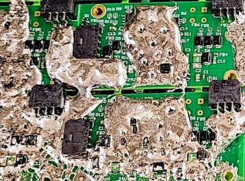
At RBB, we run both lead and RoHS wave soldering processes using two Electrovert VectraES systems. Because we build a wide variety of assemblies, our team regularly works through the variables that can make the difference between a clean wave-soldered PCBA and a difficult one.
So, what causes flooding and what can you do about it?
What Causes Solder Flooding During Wave Soldering?
Wave soldering sounds straightforward: flux the board, preheat it, pass the solder side across a controlled wave of molten solder, and create the required solder joints.
In practice, a lot is happening in a very short period of time.
Board design, component orientation, solder mask, lead length, flux application, conveyor speed, preheat profile, solder-wave height, board angle, pallet design, and even component geometry can affect the outcome.
When those variables aren't working together, molten solder can travel farther than intended or fail to release cleanly from the assembly.
The result can range from a few solder bridges to the extreme flooding shown in our example photo.
DO: Design With the Wave Process in Mind
One of the best ways to prevent wave solder problems is to consider Design for Manufacturability (DFM) before production begins. Component placement and orientation matter. Closely spaced leads, connectors positioned in difficult orientations, insufficient solder-mask clearances, and components that interfere with proper solder drainage can all make an assembly more challenging to process.
If an assembly will be wave soldered, involve your electronics manufacturing partner early.
At RBB, we'd much rather identify a potential manufacturing problem while we're reviewing a print, Gerber file, or prototype than discover it after production has started. A relatively small design or process adjustment can sometimes prevent a much larger quality problem later.
DON'T: Assume More Solder Means a Better Joint
It doesn't.
A good through-hole solder joint needs proper hole fill and wetting—not the largest possible amount of solder.
Increasing wave height or contact time in an attempt to correct insufficient soldering can introduce an entirely different set of problems. Excessive contact with the solder wave can increase the opportunity for solder to reach areas that should remain protected.
Wave parameters need to be controlled, not simply increased until a joint looks full.
This is where documented process settings, experienced operators, and inspection become especially important.
DO: Pay Attention to Flux and Preheat
Flux is a critical part of the wave soldering process. It removes oxides and helps molten solder wet the surfaces that need to be soldered.
But flux application and preheat have to work together.
Too little flux can contribute to poor wetting. Too much or improperly activated flux can create other process problems. Likewise, the board needs an appropriate thermal profile before it reaches the solder wave.
The goal is repeatability: applying the correct amount of flux and consistently achieving the process temperatures required for the particular assembly.
That becomes especially important in a high-mix manufacturing environment where one PCBA may behave very differently from the next.
DON'T: Ignore Solder Mask Condition and Coverage
Solder mask isn't just there to make the board green.
It plays an important role in controlling where solder can and cannot flow.
Missing, damaged, improperly specified, or poorly registered solder mask can expose copper and provide molten solder with a path into areas where it was never intended to go.
If you're experiencing recurring solder bridges or flooding in the same location, don't automatically assume the wave solder machine is the problem. Look at the bare board, too.
Sometimes the manufacturing process is revealing an upstream PCB design or fabrication issue.
DO: Use the Right Tooling
Not every assembly should simply be placed directly onto a wave conveyor.
Wave solder pallets and selective masking can protect areas of a PCBA that should not be exposed to molten solder. Proper tooling can be especially valuable for mixed-technology assemblies containing both through-hole and surface-mount components.
But the tooling itself needs to be designed correctly.
Openings, clearances, drainage, board support, component interference, and thermal characteristics all matter. Poorly designed tooling can contribute to solder accumulation rather than preventing it.
Good tooling should make the process more repeatable.
DON'T: Treat Every PCBA the Same
This is particularly important in the type of manufacturing RBB does.
A process that works beautifully on one board isn't automatically appropriate for another.
A thick, high-copper PCB may require different thermal considerations than a smaller, lighter board. Connector-heavy assemblies may behave differently from boards with relatively few through-hole components. Lead-free solder also behaves differently from traditional leaded solder.
That's why RBB maintains dedicated capabilities for both lead and RoHS processing rather than treating wave soldering as a one-setting-fits-all operation.
DO: Control the Entire Process
Preventing solder flooding is ultimately about process control.
That means paying attention to the complete picture:
- PCB design and solder-mask integrity
- Component placement and orientation
- Lead protrusion
- Flux type and application
- Preheat profile
- Conveyor speed and angle
- Wave height and solder contact
- Solder alloy and temperature
- Pallet and masking design
- Inspection and feedback after soldering
When a defect occurs, the answer shouldn't be to immediately start changing settings at random. The better approach is to determine why it happened, identify the contributing variables, make a controlled adjustment, and verify the result.
That philosophy connects directly to one of RBB's core values: Always Better.
Continuous improvement isn't about pretending problems never happen. It's about learning from what the process is telling us and finding a better, more repeatable way to build the next assembly. RBB's external materials similarly describe that commitment as continually assessing manufacturing processes to improve efficiency and customer benefit.
DON'T: Wait Until Production to Talk About Manufacturability
This may be the biggest takeaway.
Many wave soldering problems can be prevented before a production order ever reaches the floor.
If you're designing a new PCBA, transferring an existing product from another manufacturer, or dealing with recurring solder defects on a legacy assembly, bring your manufacturing partner into the conversation.
Sometimes the solution is a process adjustment. Sometimes it's better tooling. Sometimes a minor PCB change can make the assembly considerably easier to manufacture. And sometimes the right answer is that conventional wave soldering isn't the best process for a particular portion of the board.
The important thing is finding that out before it becomes an expensive quality problem.
When Your Assembly Is Difficult, That's When Partnership Matters
RBB specializes in recurring, mission-critical PCB and industrial control panel assemblies, including products that don't always fit neatly into conventional high-volume manufacturing models. That means we're accustomed to changeovers, unusual assemblies, legacy products, and manufacturing challenges that require people to stop and think rather than simply push another board down the line.
Our goal isn't just to solder your board. It's to help you build it reliably.
That's part of what Built for Partnership. Proven Through Performance. means to us. Quality you can trust, responsive communication, engineering collaboration, and reliable delivery all start with understanding the product we're building—and being willing to move heaven and earth when a manufacturing challenge needs to be solved. RBB's commitment to quality, reliability, and continuous improvement is also reflected in our AS9100 certification.
If you're experiencing wave soldering problems, transferring a difficult assembly, or simply want another set of eyes on a PCBA before it goes into production, send us a print for review. We'd be happy to take a look and talk through how we can help.