Design for Manufacturability
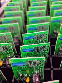
 Design for Manufacturability (DFM) is the process of designing your product so that it can be produced easily and quickly. A few adjustments can help you get your new product to market before your competition, and help you meet your delivery schedules! The fewer steps in the electronics manufacturing process means less time between ordering and receiving your product.
Steps In Manufacturing
Fewer “steps” in the manufacturing process means less time between ordering and receiving your product. So, what is a “step” in electronics manufacturing?
A “step” is each time a product is required to be handled, moved, turned over, and placed in a fixture or machine. By knowing and utilizing DFM, you minimize the number of steps needed to produce your product.
Why is DFM often missed or not applied in the design stage of your products? A Design Engineers’ primary goal is how your product functions not how it will be produced. It's more exciting to add bells and whistles than it is to design for ease of manufacturing.
RBB recommends several DFM step reductions for designing a Printed Circuit Board (PCB):
RBB recommends several DFM step reductions for designing a PCB:
1. The PCB Bare Board:
- If possible, make the shape of the board a rectangle or square. Odd shaped boards will cost more and take more steps to produce.
2. Components:
- Minimize the number of different components.
- (Example: Use the same value of Cap or Resistor wherever you can)
- Choose components that are available without long lead times or are not hard to find.
- Choose active components. Obsolete components will cost more, and availability cannot be predicted.
- Choose components that can have more than one manufacturer and include them in your Bill of Material.
- Minimize Components that cannot be washed after soldering (non-sealed components that cannot get wet). This will reduce the need for manual soldering and cleaning.
3. Layout of the Circuit Board:
 If possible, keep components at least 5mm away from the edge of the board. The edge of the board is needed to hold and move the board through all process equipment. Components too close will have to be placed later by hand and increase labor cost.
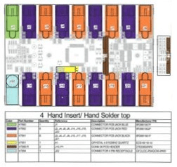
- Keep all components to the top side of the board. A board with components on both sides must go through the process twice; increasing handling and labor time, which equates to cost!
- Components with polarity should be marked clearly on the silkscreen.
Bottom line!
Non-value-added labor cost that can be reduced by using Design for Manufacturability in the design and prototype stages of your product saves time, money, and eliminates opportunities for error.
These are just a few recommendations for DFM. If RBB or I can help guide you through the Design for Manufacturability process, please contact us. You can also check out our different engineering support recommendations and services here.
Does your company use DFM? How has your electronics manufacturing business addressed manufacturability on new products for quality and cost issues? Let me know below!
To dig a little deeper on this topic, and learn more about other ways to save money in the high-mix, low-volume world, register to attend RBB's lunch & learn series.
For over 35 years, Steve has been a part of the RBB family in positions ranging from Service Manager, Testing Manager, Quality Manager and various engineering roles. Steve also enjoys problem solving, traveling, farming, amateur radio, collecting antique radios and leisurely walks to the refrigerator.
This post was originally published June 5, 2013.


